The Project:
Even as Moore’s Law approaches its physical limits, the demand for computational power (driven by AI and machine learning) continues to rise. To address this bottleneck, researchers are looking toward neuromorphic computing: modeling hardware after the human brain, which is exponentially more energy-efficient than traditional CPUs.
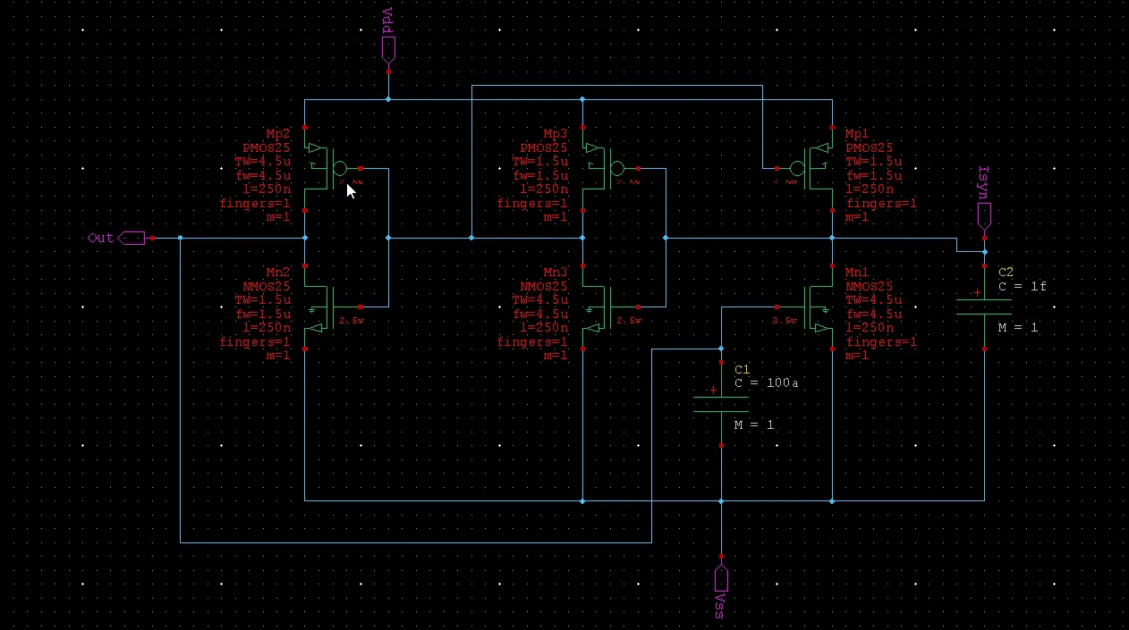
For this project, I designed, simulated, and laid out a Morris-Lecar spiking neuron model at the transistor level. The goal was to replicate the biological “firing” of a neuron using low-level circuitry and analyze its energy efficiency under various voltage conditions.
Circuit Design (Schematic)
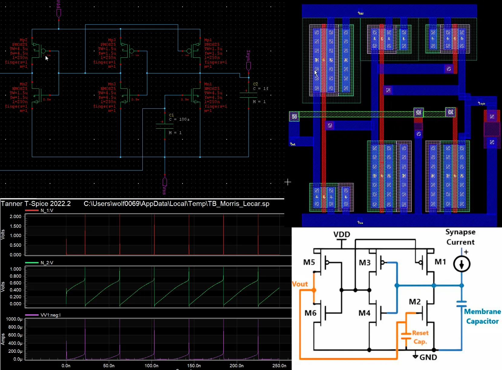
I utilized S-Edit to design the transistor-level schematic based on the Morris-Lecar biological model, which oscillates between a depolarized active phase and a hyperpolarized silent phase.
Key Design Decisions
-
Architecture: The design utilizes a 250nm architecture.
-
Transistor Sizing: The sizing ratios were critical for functionality. I used a 3:1 sizing ratio for the Mp2/Mn2 pair to enable “depolarization” (reset), and a 1:3 ratio for the Mp3/Mn3 and Mp1/Mn1 pairs to enable “hyperpolarization”.
-
Capacitance Tuning: Precise capacitance was required to control the spiking pattern. Through experimentation, I determined that a factor of 10 difference between the membrane capacitance and reset capacitance was optimal. If the reset capacitance was too large, the charge time would prevent output spiking; if the membrane capacitance was too large, it would slow the feedback signal.
Simulation & Analysis
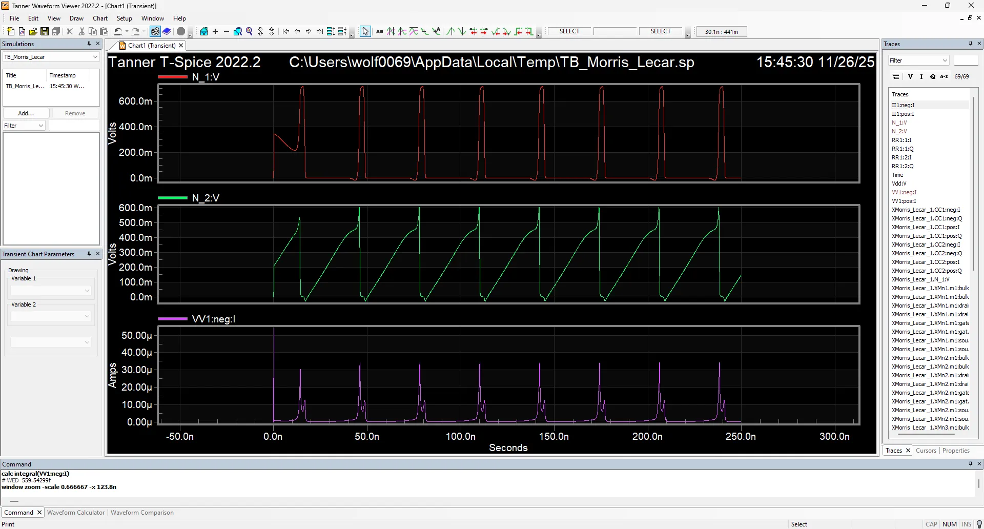
To verify the design and test for energy efficiency, I built a testbench in S-Edit that allowed me to sweep the input voltage (Vin) and measure the system’s response. I performed a transient sweep analysis (0ns to 250ns) at three distinct voltage levels: 0.7V, 2.3V, and 4V.
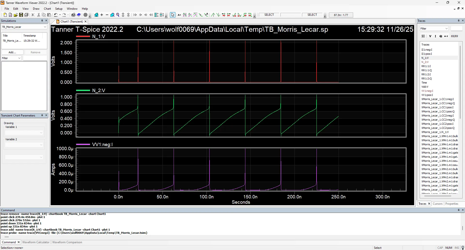
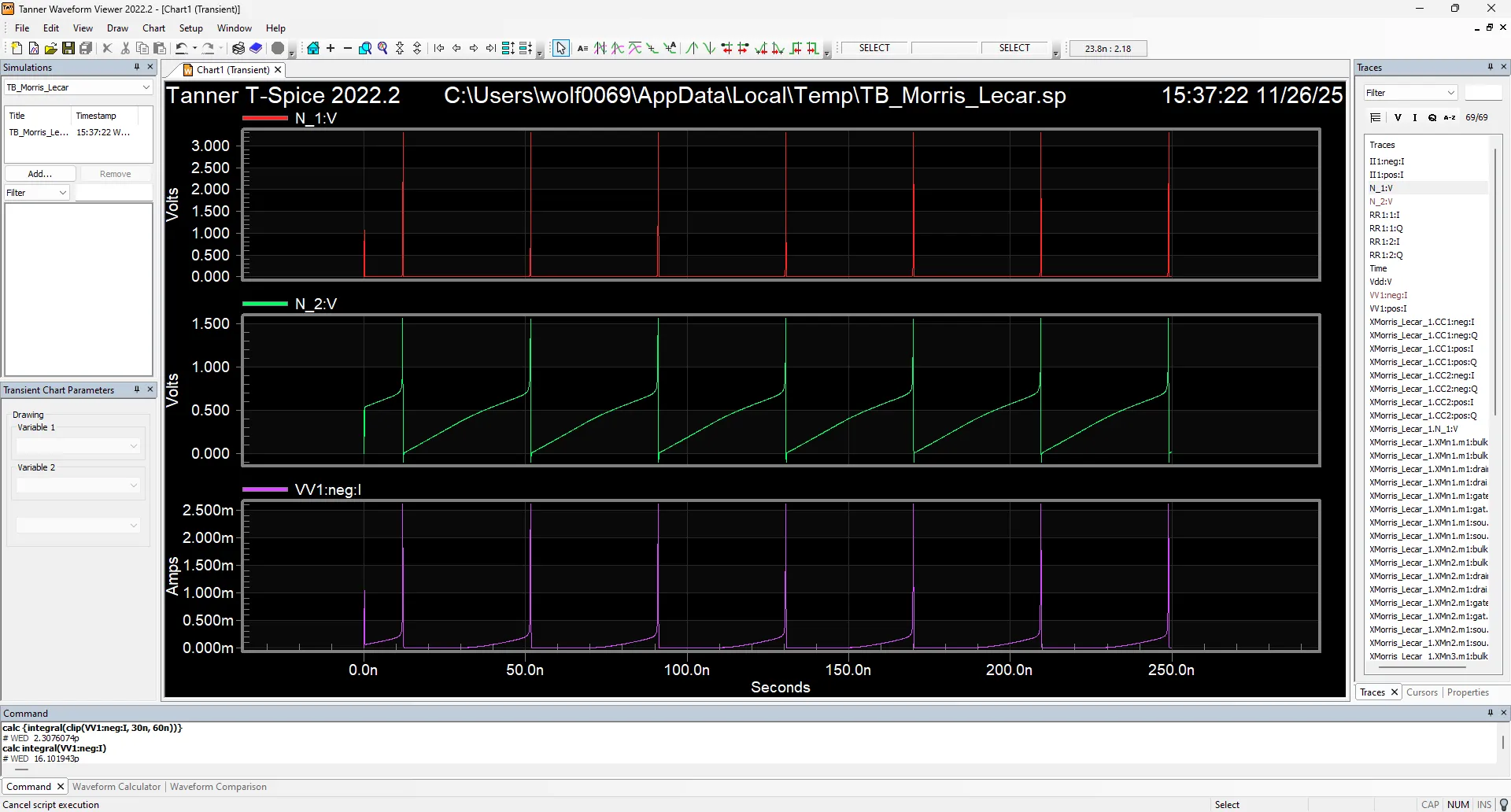
Efficiency Results
I calculated the energy consumed per spike and the average energy consumption for each voltage level by integrating the supply current over time.
| Supply Voltage | Energy Per Spike | Total Energy (250ns) | Efficiency (Vout / Vin) |
|---|---|---|---|
| 0.7V | 48.578 fJ | 391.680 fJ | 89.3% |
| 2.3V | 2.728 pJ | 16.612 pJ | 91.3% |
| 4.0V | 9.230 pJ | 64.408 pJ | 82.5% |
Conclusion
While the 0.7V circuit consumed the least energy, it failed to produce clean spikes. The 4V circuit had high power consumption with lower efficiency. The 2.3V input was determined to be the optimal solution, balancing high efficiency (91.3%) with clean output signal generation.
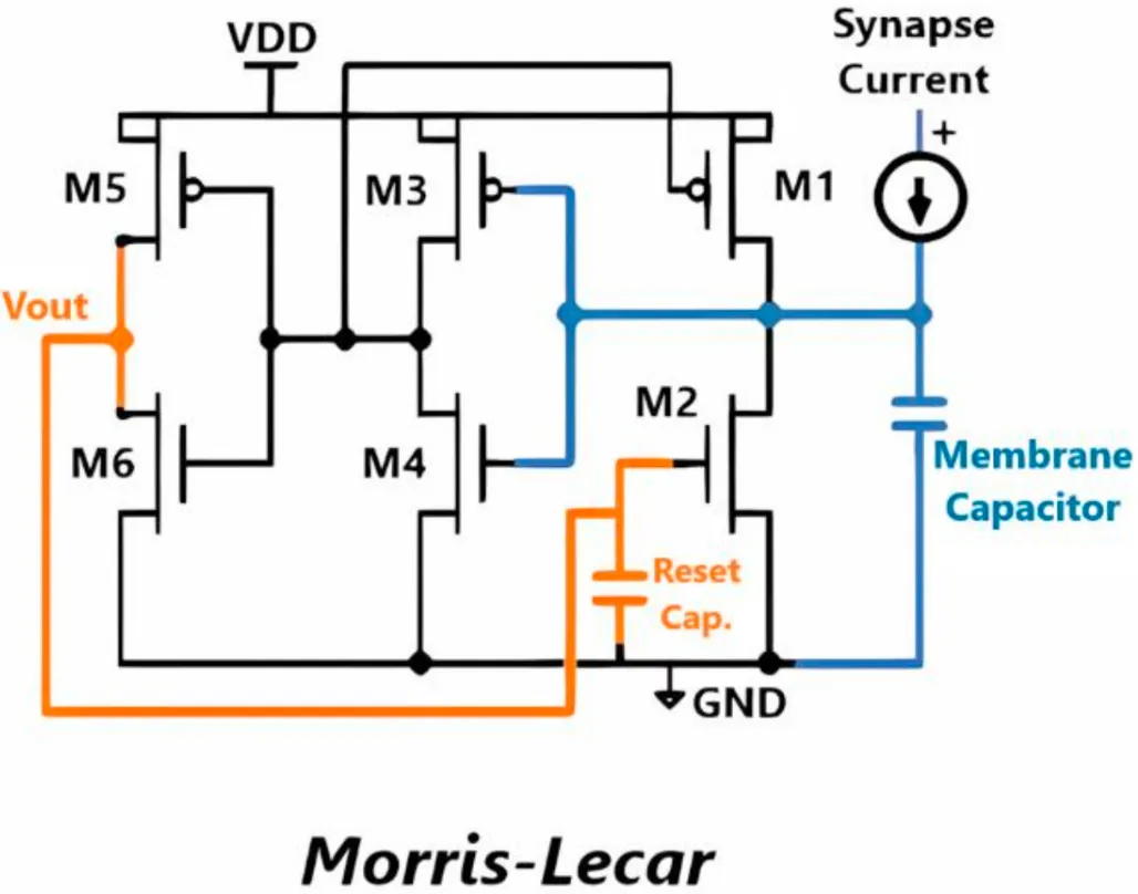
Physical Layout (L-Edit)
After verifying the schematic, I implemented the physical layout of the cell using L-Edit. This process involved translating the schematic into physical layers (Poly, Metal1, Metal2, N-Wells) while adhering to strict Design Rule Checks (DRC).
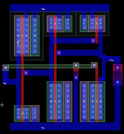
Layout Challenges
-
Compact Design: The overall layout size was constrained to 14.875 by 15.600 microns.
-
Routing: I prioritized Metal1 connections but utilized vias to Metal2 for connecting the gate of Mn3 to the positive node of C1 to simplify routing.
-
Capacitor Implementation: Capacitors were constructed using Poly1 and Poly2 layers. I ensured the membrane capacitor was physically larger than the reset capacitor to reflect the schematic values.
I performed rigorous DRC verification to ensure all metal traces met minimum sizing requirements and that via stacks (Metal1-Metal2-Poly) were properly connected without “redlining” errors.
Conclusion
This project provided a comprehensive overview of the VLSI design flow, from low-level schematic design in S-Edit to simulation in Waveform Viewer and physical layout in L-Edit. I successfully demonstrated that biologically inspired circuits can be simulated with standard CMOS technology, bridging the gap between biological efficiency and silicon-based hardware.
Moving forward, I plan to explore how complex logic can be implemented by networking multiple Morris-Lecar cells together.